(Hong Kong)

Product Summary
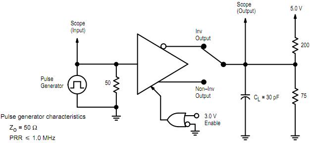
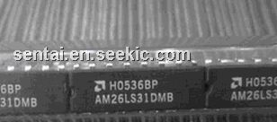
The AM26LS31DMB is a quad differential line driver. The AM26LS31DMB intended for digital data transmission over balanced lines. The AM26LS31DMB meets all the requirements of EIA–422 Standard and Federal Standard 1020. The AM26LS31DMB provides an enable/disable function common to all four drivers as opposed to the split enables on the MC3487 EIA–422 driver.
Parametrics
AM26LS31DMB absolute maximum ratings: (1)Power Supply Voltage, VCC: 8.0 Vdc; (2)Input Voltage, VI: 5.5 Vdc; (3)Operating Ambient Temperature Range, TA: 0 to + 70 ℃; (4)Operating Junction Temperature Range, TJ: 150 ℃; (5)Storage Temperature Range, Tstg: –65 to + 150 ℃; (6)Input Voltage – Low Logic State, VIL: 0.8 Vdc; (7)Input Voltage – High Logic State, VIH: 2.0 Vdc; (8)Input Current – Low Logic State, IIL: 360 μA; (9)Input Current – High Logic State, IIH: +20 μA; (10)Input Clamp Voltage, VIK: 1.5 V; (11)Output Voltage – Low Logic State, VOL: 0.5 V; (12)Output Voltage – High Logic State, VOH: 2.5 V; (13)Output Short Circuit Current, IOS: –30 to 150 mA; (14)Output Leakage Current – Hi–Z State, IO(Z): 20 μA; (15)Output Leakage Current – Power OFF, IO(off): + 100 μA; (16)Output Offset Voltage Difference, Note 2, VOS – VOS: ±0.4 V; (17)Output Differential Voltage, Note 2, VOD: 2.0 V; (18)Output Differential Voltage Difference, Note 2, VOD: ±0.4 V; (19)Power Supply Current, ICCX: –60 to 80 mA.
Features
AM26LS31DMB features: (1)Full EIA–422 Standard Compliance; (2)Single +5.0 V Supply; (3)Meets Full VO = 6.0 V, VCC = 0 V, IO < 100 μA Requirement; (4)Output Short Circuit Protection; (5)Complementary Outputs for Balanced Line Operation; (6)High Output Drive Capability; (7)Advanced LS Processing; (8)PNP Inputs for MOS Compatibility.
Diagrams